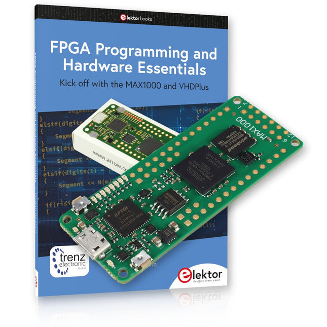
Einstieg in die FPGA-Programmierung mit dem MAX1000-Board und VHDPlus
Sind Sie bereit, die FPGA-Programmierung zu meistern? Mit diesem Bundle tauchen Sie ein in die Welt der Field-Programmable Gate Arrays (FPGAs) – einer konfigurierbaren integrierten Schaltung, die nach der Herstellung programmiert werden kann. Verwirklichen Sie jetzt Ihre Ideen, von einfachen Projekten bis hin zu kompletten Mikrocontrollersystemen!
Das MAX1000 ist ein kompaktes und leistungsstarkes FPGA-Entwicklungsboard mit zahlreichen Funktionen wie Speicher, Benutzer-LEDs, Drucktasten und flexiblen I/O-Ports. Es ist der ideale Ausgangspunkt für alle, die mehr über FPGAs und Hardwarebeschreibungssprachen (HDLs) erfahren möchten.
Mit dem beiliegenden Buch "FPGA Programming and Hardware Essentials" erhalten Sie einen praktischen Einblick in die Programmiersprache VHDPlus – eine einfachere Version von VHDL. Sie arbeiten mit dem MAX1000 an praktischen Projekten und erwerben so die Fähigkeiten und das Selbstvertrauen, um Ihrer Kreativität freien Lauf zu lassen.
Enthaltene Projekte im Buch
Arduino-gesteuerter BCD-zu-7-Segment-Display-Decoder
Verwenden Sie einen Arduino Uno R4, um BCD-Daten an den Decoder zu liefern, wobei von 0 bis 9 mit einer Verzögerung von einer Sekunde gezählt wird.
Multiplexierter 4-stelliger Ereigniszähler
Erstellen Sie einen Ereigniszähler, der die Gesamtzahl auf einem 4-stelligen Display anzeigt und sich mit jedem Tastendruck erhöht
PWM-Wellenform mit festem Arbeitszyklus
Erzeugen Sie eine PWM-Wellenform mit 1 kHz und einem festen Arbeitszyklus von 50 %
Ultraschall-Abstandsmessung
Messen Sie Entfernungen mit einem Ultraschallsensor und zeigen Sie die Ergebnisse auf einer 4-stelligen 7-Segment-LED an
Elektronisches Schloss
Bauen Sie ein einfaches elektronisches Schloss mit kombinatorischen Logikgattern mit Druckknöpfen und einem LED-Ausgang
Temperatursensor
Überwachen Sie die Umgebungstemperatur mit einem TMP36-Sensor und zeigen Sie die Messwerte auf einer 7-Segment-LED an
MAX1000 FPGA Development Board
Das MAX1000 ist ein anpassbares IoT/Maker-Board, das zur Evaluierung, Entwicklung und/oder Verwendung in einem Produkt bereit ist. Es basiert auf dem Intel MAX10 FPGA, dem branchenweit ersten nichtflüchtigen programmierbaren Logikgerät (PLDs) mit einem Chip, das den optimalen Satz an Systemkomponenten integriert.
Benutzer können jetzt die Vorteile einer enormen Rekonfigurierbarkeit gepaart mit einem leistungsstarken FPGA-System mit geringem Stromverbrauch nutzen. MAX10-Geräte bieten intern gespeicherte Dual-Images mit Selbstkonfiguration, umfassende Designschutzfunktionen, integrierte ADCs und Hardware zur Implementierung des Nios II 32-Bit-Mikrocontroller-IP und sind ideale Lösungen für Systemmanagement, Protokollüberbrückung, Kommunikationssteuerungsebenen, Industrie, Automobil- und Verbraucheranwendungen.
Der MAX1000 ist mit einem Arrow USB-Programmierer2, SDRAM, Flash-Speicher, Beschleunigungssensor und PMOD/Arduino-MKR-Anschlüssen ausgestattet, was ihn zu einer voll ausgestatteten Plug-and-Play-Lösung ohne zusätzliche Kosten macht.
Technische Daten
MAX 10
8 kLE
- Flash
Dual innen
- ADC
8x 12 Bit
- Temperaturbereich
0~85°C
- Versorgung
USB/Pins
SDRAM
8 MB
3-Achsen-MEMS
LIS3DH
USB-Programmer
an Bord
MEMS-Oszillator
12 MHz
Schalter/LED
2x / 8x
Inhalt des Bundles
Buch: FPGA Programming and Hardware Essentials (Einzelpreis: 40 €)
MAX1000 FPGA Development Board (Einzelpreis: 45 €)
Downloads
Software
Der LuckFox Pico Ultra ist ein kompakter Single-Board-Computer (SBC) mit dem Rockchip RV1106G3-Chipsatz, der für KI-Verarbeitung, Multimedia und stromsparende Embedded-Anwendungen entwickelt wurde.
Er ist mit einer integrierten 1-TOPS-NPU ausgestattet und eignet sich daher ideal für Edge-KI-Workloads. Mit 256 MB RAM, 8 GB Onboard-eMMC-Speicher, integriertem WLAN und Unterstützung für das LuckFox PoE-Modul bietet das Board Leistung und Vielseitigkeit für eine Vielzahl von Anwendungsfällen.
Der LuckFox Pico Ultra läuft unter Linux und unterstützt eine Vielzahl von Schnittstellen – darunter MIPI CSI, RGB-LCD, GPIO, UART, SPI, I²C und USB – und bietet so eine einfache und effiziente Entwicklungsplattform für Anwendungen in den Bereichen Smart Home, Industriesteuerung und IoT.
Technische Daten
Chip
Rockchip RV1106G3
Prozessor
Cortex-A7 1,2 GHz
Neuronaler Netzwerkprozessor (NPU)
1 TOPS, unterstützt int4, int8, int16
Bildprozessor (ISP)
Max. Eingangsgeschwindigkeit 5 M @30fps
Speicher
256 MB DDR3L
WLAN + Bluetooth
2,4 GHz WiFi-6 Bluetooth 5.2/BLE
Kameraschnittstelle
MIPI CSI 2-Lane
DPI-Schnittstelle
RGB666
PoE-Schnittstelle
IEEE 802.3af PoE
Lautsprecherschnittstelle
MX1,25 mm
USB
USB 2.0 Host/Gerät
GPIO
30 GPIO Pins
Ethernet
10/100M Ethernet-Controller und eingebetteter PHY
Standardspeichermedium
eMMC (8 GB)
Lieferumfang
1x LuckFox Pico Ultra W
1x LuckFox PoE Modul
1x IPX 2,4G 2 dB Antenne
1x USB-A auf USB-C Kabel
1x Schraubensatz
Downloads
Wiki
Kick off with the MAX1000 and VHDPlus
Ready to Master FPGA Programming? In this guide, we’re diving into the world of Field Programmable Gate Arrays (FPGAs) – a configurable integrated circuit that can be programmed after manufacturing. Imagine bringing your ideas to life, from simple projects to complete microcontroller systems!
Meet the MAX1000: a compact and budget-friendly FPGA development board packed with features like memory, user LEDs, push-buttons, and flexible I/O ports. It’s the ideal starting point for anyone wanting to learn about FPGAs and Hardware Description Languages (HDLs).
In this book, you’ll get hands-on with the VHDPlus programming language – a simpler version of VHDL. We’ll work on practical projects using the MAX1000, helping you gain the skills and confidence to unleash your creativity.
Get ready for an exciting journey! You’ll explore a variety of projects that highlight the true power of FPGAs. Let’s turn your ideas into reality and embark on your FPGA adventure – your journey starts now!
Exciting Projects You’ll Find in This Book
Arduino-Driven BCD to 7-Segment Display Decoder
Use an Arduino Uno R4 to supply BCD data to the decoder, counting from 0 to 9 with a one-second delay
Multiplexed 4-Digit Event Counter
Create an event counter that displays the total count on a 4-digit display, incrementing with each button press
PWM Waveform with Fixed Duty Cycle
Generate a PWM waveform at 1 kHz with a fixed duty cycle of 50%
Ultrasonic Distance Measurement
Measure distances using an ultrasonic sensor, displaying the results on a 4-digit 7-segment LED
Electronic Lock
Build a simple electronic lock using combinational logic gates with push buttons and an LED output
Temperature Sensor
Monitor ambient temperature with a TMP36 sensor and display the readings on a 7-segment LED
Downloads
Software
Das ATmega328 Uno Development Board (Arduino Uno kompatibel) ist ein Mikrocontroller-Board, das auf dem ATmega328 basiert.
Es verfügt über 14 digitale Ein-/Ausgangspins (von denen 6 als PWM-Ausgänge verwendet werden können), 6 analoge Eingänge, einen 16 MHz-Keramikresonator, einen USB-Anschluss, eine Strombuchse, einen ICSP-Header und eine Reset-Taste.
Es enthält alles, was zur Unterstützung des Mikrocontrollers erforderlich ist. Schließen Sie es über ein USB-Kabel an einen Computer an oder betreiben Sie es mit einem AC-DC-Adapter oder einer Batterie, um loszulegen.
Technische Daten
Mikrocontroller
ATmega328
Betriebsspannung
5 V DC
Eingangsspannung (empfohlen)
7-12 V DC
Eingangsspannung (Grenzwerte)
6-20 V DC
Digitale I/O-Pins
14 (davon 6 mit PWM-Ausgang)
Analoge Eingangspins
6
SRAM
2 kB (ATmega328)
EEPROM
1 kB (ATmega328)
Flash-Speicher
32 kB (ATmega328), davon 0,5 kB vom Bootloader verwendet
Taktgeschwindigkeit
16 MHz
Downloads
Manual
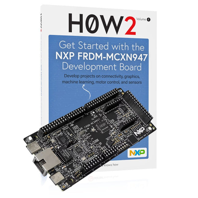
The FRDM-MCXN947 is a compact and versatile development board designed for rapid prototyping with MCX N94 and N54 microcontrollers. It features industry-standard headers for easy access to the MCU's I/Os, integrated open-standard serial interfaces, external flash memory, and an onboard MCU-Link debugger.
Technische Daten
Microcontroller
MCX-N947 Dual Arm Cortex-M33 cores @ 150 MHz each with optimized performance efficiency, up to 2 MB dual-bank flash with optional full ECC RAM, External flash
Accelerators: Neural Processing Unit, PowerQuad, Smart DMA, etc.
Memory Expansion
*DNP Micro SD card socket
Connectivity
Ethernet Phy and connector
HS USB-C connectors
SPI/I²C/UART connector (PMOD/mikroBUS, DNP)
WiFi connector (PMOD/mikroBUS, DNP)
CAN-FD transceiver
Debug
On-board MCU-Link debugger with CMSIS-DAP
JTAG/SWD connector
Sensor
P3T1755 I³C/I²C Temp Sensor, Touch Pad
Expansion Options
Arduino Header (with FRDM expansion rows)
FRDM Header
FlexIO/LCD Header
SmartDMA/Camera Header
Pmod *DNP
mikroBUS
User Interface
RGB user LED, plus Reset, ISP, Wakeup buttons
Lieferumfang
1x FRDM-MCXN947 Development Board
1x USB-C Cable
1x Quick Start Guide
Downloads
Datasheet
Block diagram
For Speed, Area, Power, and Reliability
This book teaches the fundamentals of FPGA operation, covering basic CMOS transistor theory to designing digital FPGA chips using LUTs, flip-flops, and embedded memories. Ideal for electrical engineers aiming to design large digital chips using FPGA technology.
Discover:
The inner workings of FPGA architecture and functionality.
Hardware Description Languages (HDL) like Verilog and VHDL.
The EDA tool flow for converting HDL source into a functional FPGA chip design.
Insider tips for reliable, low power, and high performance FPGA designs.
Example designs include:
Computer-to-FPGA UART serial communication.
An open-source Sump3 logic analyzer implementation.
A fully functional graphics controller.
What you need:
Digilent BASYS3 or similar FPGA eval board with an AMD/Xilinx FPGA.
Vivado EDA tool suite (available for download from AMD website free of charge).
Project source files available from author’s GitHub site.
Dieses Bundle enthält:
Buch: Get Started with the NXP FRDM-MCXN947 Development Board (Einzelpreis: 40 €)
NXP FRDM-MCXN947 Development Board (Einzelpreis: 30 €)
Buch: Get Started with the NXP FRDM-MCXN947 Development Board
Projekte zu Konnektivität, Grafik, maschinellem Lernen, Motorsteuerung und Sensoren entwickeln
Dieses (englischsprachige) Buch behandelt die Verwendung des FRDM-MCXN947 Development Boards, entwickelt von NXP Semiconductors. Es integriert den Dual Arm Cortex-M33, der mit bis zu 150 MHz arbeitet. Ideal für industrielle, IoT- und maschinelles Lernen-Anwendungen. Es verfügt über Hi-Speed USB, CAN 2.0, I³C und 10/100 Ethernet. Das Board beinhaltet einen integrierten MCU-Link-Debugger, FlexI/O zur Steuerung von LCDs und Dual-Bank-Flash für Lese-und-Schreib-Operationen, mit Unterstützung für große externe serielle Speicherkonfigurationen.
Eine der wichtigen Funktionen des Entwicklungsboards ist die integrierte eIQ Neutron Neural Processing Unit (NPU), die es den Nutzern ermöglicht, AI-basierte Projekte zu entwickeln. Das Entwicklungsboard unterstützt auch Arduino Uno-Header-Pins, was es mit vielen Arduino-Shields kompatibel macht, sowie einen mikroBUS-Anschluss für MikroElektronika Click Boards und einen Pmod-Anschluss.
Ein weiterer Vorteil des FRDM-MCXN947 Development Boards ist, dass es mehrere integrierte Debug-Probes enthält, die es Programmierern ermöglichen, ihre Programme direkt mit dem MCU zu debuggen. Mit Hilfe des Debuggers können Programmierer Schritt für Schritt durch ein Programm gehen, Breakpoints setzen, Variablen ansehen und ändern, und vieles mehr.
Im Buch wurden viele funktionierende und getestete Projekte mit der beliebten MCUXpresso IDE und dem SDK unter Verwendung verschiedener Sensoren und Aktoren entwickelt. Auch die Verwendung der populären CMSIS-DSP-Bibliothek wird anhand mehrerer häufig genutzter Matrixoperationen erklärt.
Die im Buch bereitgestellten Projekte können ohne Änderungen in vielen Anwendungen eingesetzt werden. Alternativ können die Leser ihre eigenen Projekte auf den im Buch vorgestellten Projekten aufbauen, während sie ihre eigenen Projekte entwickeln.
NXP FRDM-MCXN947 Development Board
TDas FRDM-MCXN947 ist ein kompaktes und vielseitiges Entwicklungsboard, das für das Rapid Prototyping mit MCX N94- und N54-Mikrocontrollern konzipiert wurde. Es verfügt über Industriestandard-Header für den einfachen Zugang zu den I/Os der MCU, integrierte serielle Schnittstellen nach offenem Standard, externen Flash-Speicher und einen Onboard-MCU-Link-Debugger.
Technische Daten
Mikrocontroller
MCX-N947 Dual Arm Cortex-M33-Kerne mit jeweils 150 MHz und optimierter Leistungseffizienz, bis zu 2 MB Dual-Bank-Flash mit optionalem Full-ECC-RAM, externer Flash
Beschleuniger: Neural Processing Unit, PowerQuad, Smart DMA usw.
Speichererweiterung
*DNP MicroSD-Kartensteckplatz
Konnektivität
Ethernet Phy und Connector
HS USB-C-Anschlüsse
SPI/I²C/UART-Anschluss (PMOD/mikroBUS, DNP)
WiFi-Anschluss (PMOD/mikroBUS, DNP)
CAN-FD-Transceiver
Debuggen
Integrierter MCU-Link-Debugger mit CMSIS-DAP
JTAG/SWD-Anschluss
Sensor
P3T1755 I³C/I²C-Temperatursensor, Touchpad
Erweiterungsoptionen
Arduino-Header (mit FRDM-Erweiterungszeilen)
FRDM-Header
FlexIO/LCD-Header
SmartDMA/Kamera-Header
Pmod *DNP
mikroBUS
Benutzeroberfläche
RGB-Benutzer-LED sowie Reset-, ISP- und Wakeup-Tasten
Lieferumfang
1x FRDM-MCXN947 Development Board
1x USB-C Kabel
1x Quick Start Guide
Downloads
Datasheet
Block diagram
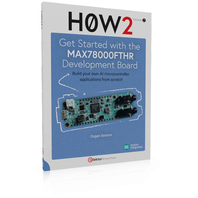
Build your own AI microcontroller applications from scratch
The MAX78000FTHR from Maxim Integrated is a small development board based on the MAX78000 MCU. The main usage of this board is in artificial intelligence applications (AI) which generally require large amounts of processing power and memory. It marries an Arm Cortex-M4 processor with a floating-point unit (FPU), convolutional neural network (CNN) accelerator, and RISC-V core into a single device. It is designed for ultra-low power consumption, making it ideal for many portable AI-based applications.
This book is project-based and aims to teach the basic features of the MAX78000FTHR. It demonstrates how it can be used in various classical and AI-based projects. Each project is described in detail and complete program listings are provided. Readers should be able to use the projects as they are, or modify them to suit their applications. This book covers the following features of the MAX78000FTHR microcontroller development board:
Onboard LEDs and buttons
External LEDs and buttons
Using analog-to-digital converters
I²C projects
SPI projects
UART projects
External interrupts and timer interrupts
Using the onboard microphone
Using the onboard camera
Convolutional Neural Network
Das OKdo E1 ist ein äußerst kostengünstiges Entwicklungsboard, das auf dem Dual-Core-Arm-Cortex-M33-Mikrocontroller LPC55S69JBD100 von NXP basiert. Das E1-Board eignet sich perfekt für industrielles IoT, Gebäudesteuerung und -automatisierung, Unterhaltungselektronik sowie allgemeine eingebettete und sichere Anwendungen.
Merkmale
Prozessor mit Arm TrustZone, Floating Point Unit (FPU) und Memory Protection Unit (MPU)
CASPER Crypto-Coprozessor zur Hardwarebeschleunigung für bestimmte asymmetrische kryptografische Algorithmen
PowerQuad Hardware Accelerator für Fest- und Gleitkomma-DSP-Funktionen
SRAM Physical Unclonable Function (PUF) zur Schlüsselgenerierung, -speicherung und -rekonstruktion
PRINCE-Modul zur Echtzeit-Verschlüsselung und Entschlüsselung von Flash-Daten
AES-256- und SHA2-Engines
Bis zu neun Flexcomm-Schnittstellen. Jede Flexcomm-Schnittstelle kann per Software als USART-, SPI-, I²C- und I²S-Schnittstelle ausgewählt werden
USB 2.0 High-Speed-Host/Geräte-Controller mit On-Chip-PHY
USB 2.0 Full-Speed Host/Geräte-Controller mit On-Chip-PHY
Bis zu 64 GPIOs Sichere digitale Ein-/Ausgabe-Kartenschnittstelle (SD/MMC und SDIO).
Spezifikationen
LPC55S69JBD100 640-KByte-Flash-Mikrocontroller
Eingebauter CMSIS-DAP v1.0.7-Debugger basierend auf LPC11U35
Interne PLL-Unterstützung für einen Betrieb mit bis zu 100 MHz, 16 MHz können für den vollen 150-MHz-Betrieb montiert werden.
SRAM 320kB
32-kHz-Quarz für Echtzeituhr
4 Benutzerschalter
3-Farben-LED
Benutzer-USB-Anschluss
2 16-polige Erweiterungsstecker
UART über USB virtueller COM-Port
Die "Field Programmable Gate Array"-Bausteine sind der moderne Weg, digitale Schaltungen schnell und effizient aufzubauen. Mit preiswerten Evaluierungskits lassen sich komplexe digitale Schaltungen realisieren, ohne auf die immer schwieriger werdende Löttechnik zurückzugreifen. Jedoch hat sich hierdurch die Beschreibung der digitalen Schaltungen geändert, womit auch die Methodik angepasst werden muss.Dieses Buch Buch gibt zunächst eine kurze Einführung in die digitale Schaltungstechnik, mit dem Schwerpunkt auf den in FPGA-Bausteinen verwendeten Grundelementen. Danach werden die Randbedingungen und Effekte, die beim Entwurf digitaler Schaltungen auftreten können, beschrieben und schließlich die Grundelemente als HDL-Beschreibungen in den Sprachen VHDL und Verilog aufgeführt. Die Methodik zum Erstellen einer FPGA-Schaltung mit den Schritten Simulation, Verifikation und Implementierung sowie die Programmwerkzeuge zur Durchführung dieser Schritte werden erläutert. Abschließend wird an dem Beispiel eines Algorithmus für einen Frequenzgenerator zur direkten digitalen Synthese das Vorgehen demonstriert.Der Autor hat sein Wissen in langjähriger Entwicklungsarbeit beim Systementwurf und in der Verifikation von ASIC-Schaltungen aufgebaut und diese Methodiken erfolgreich bei der Implementierung von Prototypen und Produkten mit FPGA-Bausteinen umgesetzt. Mit diesem Buch möchte er die praktischen Erfahrungen zusammenfassen und in kompakter Form weitergeben.
The EC200U-EU C4-P01 development board features the EC200U-EU LTE Cat 1 wireless communication module, offering a maximum data rate of up to 10 Mbps for downlink and 5 Mbps for uplink. It supports multi-mode and multi-band communication, making it a cost-effective solution.
The board is designed in a compact and unified form factor, compatible with the Quectel multi-mode LTE Standard EC20-CE. It includes an onboard USB-C port, allowing for easy development with just a USB-C cable.
Additionally, the board is equipped with a 40-pin GPIO header that is compatible with most Raspberry Pi HATs.
Features
Equipped with EC200U-EU LTE Cat 1 wireless communication module, multi-mode & multi-band support
Onboard 40-Pin GPIO header, compatible with most Raspberry Pi HATs
5 LEDs for indicating module operating status
Supports TCP, UDP, PPP, NITZ, PING, FILE, MQTT, NTP, HTTP, HTTPS, SSL, FTP, FTPS, CMUX, MMS protocols, etc.
Supports GNSS positioning (GPS, GLONASS, BDS, Galileo, QZSS)
Onboard Nano SIM card slot and eSIM card slot, dual card single standby
Onboard MIPI connector for connecting MIPI screen and is fully compatible with Raspberry Pi peripherals
Onboard camera connector, supports customized SPI cameras with a maximum of 300,000 pixels
Provides tools such as QPYcom, Thonny IDE plugin, and VSCode plugin, etc. for easy learning and development
Comes with online development resources and manual (example in QuecPython)
Technische Daten
Applicable Regions
Europe, Middle East, Africa, Australia, New Zealand, Brazil
LTE-FDD
B1, B3, B5, B7, B8, B20, B28
LTE-TDD
B38, B40, B41
GSM / GPRS / EDGE
GSM: B2, B3, B5, B8
GNSS
GPS, GLONASS, BDS, Galileo, QZSS
Bluetooth
Bluetooth 4.2 (BR/EDR)
Wi-Fi Scan
2.4 GHz 11b (Rx)
CAT 1
LTE-FDD: DL 10 Mbps; UL 5 Mbps
LTE-TDD: DL 8.96 Mbps; UL 3.1 Mbps
GSM / GPRS / EDGE
GSM: DL 85.6 Kbps; UL 85.6 Kbps
USB-C Port
Supports AT commands testing, GNSS positioning, firmware upgrading, etc.
Communication Protocol
TCP, UDP, PPP, NITZ, PING, FILE, MQTT, NTP, HTTP, HTTPS, SSL, FTP, FTPS, CMUX, MMS
SIM Card
Nano SIM and eSIM, dual card single standby
Indicator
P01: Module Pin 1, default as EC200A-XX PWM0
P05: Module Pin 5, NET_MODE indicator
SCK1: SIM1 detection indicator, lights up when SIM1 card is inserted
SCK2: SIM2 detection indicator, lights up when SIM2 card is inserted
PWR: Power indicator
Buttons
PWK: Power ON/OFF
RST: Reset
BOOT: Forcing into firmware burning mode
USB ON/OFF: USB power consumption detection switch
Antenna Connectors
LTE main antenna + DIV / WiFi (scanning only) / Bluetooth antenna + GNSS antenna
Operating Temperature
−30~+75°C
Storage Temperature
−45~+90°C
Downloads
Wiki
Quectel Resources
The CubeCell series is designed primarily for LoRa/LoRaWAN node applications.
Built on the ASR605x platform (ASR6501, ASR6502), these chips integrate the PSoC 4000 series MCU (ARM Cortex-M0+ Core) with the SX1262 module. The CubeCell series offers seamless Arduino compatibility, stable LoRaWAN protocol operation, and straightforward connectivity with lithium batteries and solar panels.
The HTCC-AB02S is a developer-friendly board with an integrated AIR530Z GPS module, ideal for quickly testing and validating communication solutions.
Features
Arduino compatible
Based on ASR605x (ASR6501, ASR6502), those chips are already integrated the PSoC 4000 series MCU (ARM Cortex M0+ Core) and SX1262
LoRaWAN 1.0.2 support
Ultra low power design, 21 uA in deep sleep
Onboard SH1.25-2 battery interface, integrated lithium battery management system (charge and discharge management, overcharge protection, battery power detection, USB/battery power automatic switching)
Good impendence matching and long communication distance
Onboard solar energy management system, can directly connect with a 5.5~7 V solar panel
Micro USB interface with complete ESD protection, short circuit protection, RF shielding, and other protection measures
Integrated CP2102 USB to serial port chip, convenient for program downloading, debugging information printing
Onboard 0.96-inch 128x64 dot matrix OLED display, which can be used to display debugging information, battery power, and other information
Using Air530 GPS module with GPS/Beidou Dual-mode position system support
Specifications
Main Chip
ASR6502 (48 MHz ARM Cortex-M0+ MCU)
LoRa Chipset
SX1262
Frequency
863~870 MHz
Max. TX Power
22 ±1 dBm
Max. Receiving Sensitivity
−135 dBm
Hardware Resource
2x UART1x SPI2x I²C1x SWD3x 12-bit ADC input8-channel DMA engine16x GPIO
Memory
128 Kb FLASH16 Kb SRAM
Power consumption
Deep sleep 21 uA
Interfaces
1x Micro USB1x LoRa Antenna (IPEX)2x (15x 2.54 Pin header) + 3x (2x 2.54 Pin header)
Battery
3.7 V lithium battery (power supply and charging)
Solar Energy
VS pin can be connected to 5.5~7 V solar panel
USB to Serial Chip
CP2102
Display
0.96" OLED (128 x 64)
Operating temperature
−20~70°C
Dimensions
55.9 x 27.9 x 9.5 mm
Included
1x CubeCell HTCC-AB02S Development Board
1x Antenna
1x 2x SH1.25 battery connector
Downloads
Datasheet
Schematic
GPS module (Manual)
Quick start
GitHub